2D materials under pressure
They are extremely thin, often only one atomic layer thick, which is why they are called “two-dimensional”: These new materials have unusual properties that make them interesting for energy applications, catalysts or sensors, for example. The challenge is to be able to produce a high material quality even on an industrial scale. Physicists at UDE have now found a method to produce two different 2D materials from a single process gas. Their study, published in ACS Nano, has model character.
The ideal two-dimensional material forms a perfect lattice with no imperfections, and there are as few grain boundaries as possible – something like seams between perfect regions created during manufacturing. One of these promising materials is hexagonal boron nitride (hBN), which consists of the elements boron (B) and nitrogen (N). Like the more familiar graphene, hBN forms a lattice, but it is an insulator, making it interesting, for example, for transistors made from multiple layers of different 2D materials.
One manufacturing method for hBN is chemical vapor deposition (CVD), which was also used by the team led by Professor Dr. Michael Horn-von Hoegen of UDE. In this process, the gaseous process gas borazine is passed over an iridium single crystal as a source of boron and nitrogen. There, the gas first decomposes and then forms a new, lattice-like structure on the iridium surface at high temperatures of up to 1,100 °C.
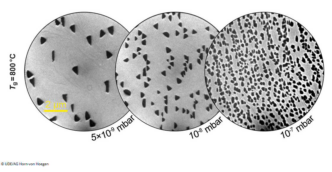
What surprised the physicists themselves was that, depending on the temperature, either hBN (800°C) or borophene (from about 950°C) forms – a lattice structure consisting of a single atomic layer of boron, analogous to graphene. In this case, the nitrogen desorbs into the surrounding high vacuum. In addition, the team found that the applied pressure in the experiment affects the growth of the material: If the pressure is too low, no coherent layer forms on the iridium; if the pressure is too high, too many individual islets form, which grow together irregularly and reduce the material quality.

In the picture: Electron micrographs of the growth of hBN at the same temperature (800°C) but different precursor gas pressure (increase from left to right). It can be seen well that the island density increases with increasing pressure.
The team succeeded in identifying the parameters that lead to a high-quality, closed layer. They also found the ideal manufacturing temperature for each of two different materials from a single precursor. “Our results have model character for other studies with bi-elemental precursors,” Horn-von Hoegen said. “They should be considered in the future for all new 2D materials created by CVD,” adds Marko Kriegel, who conducted the study for his master’s thesis.
There is not yet an efficient way to separate the material from the expensive iridium crystal, but the results can be transferred to CVD processes with other, less expensive substrates that could be etched away, for example.
Text by Birte Vierjahn, Press Resort University of Duisburg-Essen
https://www.uni-due.de/2023-10-04-2d-materialien-unter-druck
We are proud that this work was done within our international research training group.
The original publication can be found here: https://doi.org/10.1021/acsnano.3c04038


